Specialists in providing scientific component solutions in circuit applications
Service hotline:0755-83048021
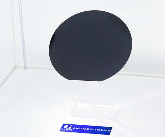
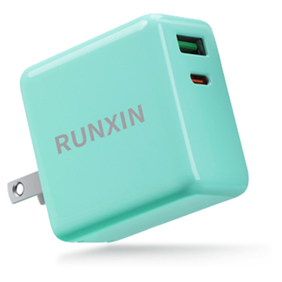
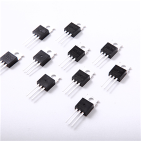
one stopComponentsSolution provider
Factory Authorised In-stock Fast delivery
氮化镓 (GaN) 外延片
  • 氮化镓 (GaN) 外延片
  • 氮化镓 (GaN) 外延片
氮化镓 (GaN) 外延片

氮化镓(GaN)外延片

润新微电子提供具有更高性价比、稳定可靠的氮化镓产品,致力于推动电能转换革命!

■ 控制生长条件实现优异的二维电子气

■ 利用特有的缓冲层生长技术实现高击穿电压和极低漏电流

■ 原位氮化硅沉积提供了优良的动态性能,提高器件可靠性

■ 控制生长条件实现的高均匀性和重复性


National Service Hotline:

0755-83048021

Key Features:

● High Vertical Breakdown Voltage: >1000V

● Low Leakage Current @Sub. Ground:<0.1uA/mm2@600V

● Bow X/Y: +/-45um

Typical Applications:

● 650V HEMTs

● 650V Diodes

Parameters Measurements
Substrate 6” 1mm <111> p-type Si
Epi ThickAvg ~5um
Epi ThickUnif <2%
Bow +/-45um
Cracking <5mm
Vertical BV >1000V
HEMT Al% 25-35%
HEMT ThickAvg 20-30nm
Insitu SiN Cap 5-60nm
2DEG conc. ~1013cm-2
Mobility ~2000cm2/Vs (<2%)
Rsh <330ohm/sq (<2%)


Related product recommendation
Contact Us
Shenzhen jingtaiyuan Technology Co., Ltd
Office address: block P, 7th floor, Sangda Yayuan, HUAFA North Road, Futian District, Shenzhen
Factory address: 501, building 2, Taiming Industrial Zone, Xinniu community, Minzhi street, Longhua District, Shenzhen
Contact: Mr. Chen
Tel: 0755-83048021
Fax: 0755-83048280
Email: schen@jghcrystal.com
QQ:2355500288
website:http://www.jtycorp.com

400-6988-056

National consultation hotline

Discover more
copyright © 2021 Shenzhen jingtaiyuan Technology Co., Ltd All rights reserved 粤ICP备14001694号-由万创科技提供技术支持